1. Circuit Technology
0) Circuit Technology
1> 1세대 : Vacuum Tube (진공관)
2> 2세대 : Transister
3> 3세대 : IC (Integrated Circuit)
chip이라고도 부릅니다.
많은 transister가 single chip내부에 있습니다.
4> 4세대 : LSI (Large Scale Integrated), VLSI (Very Large Scale Integrated)
수백만의 transister가 single chip 내부에 있습니다.
※ 결론 : 트랜지스터가 발달해서 컴퓨터가 발달할 수 있었습니다.
cf> Terminology

cf > 동그란 모양 = 0 들어와야 연결 = p-type -> closed switch = NC -> output 1 = F1 Circuit
1) Switch Models for MOS Transistors
0> Mos Transistor

Gate로 input signal(전압)이 들어온다.
→ Gate oxide(산화막)으로 전자가 들어와서 전류가 통한다. (switch 역할)
1> p-Channel (pMos Transistor, pnp Transistor, Normally Closed Switch Contact, NC)
(동그란 모양을 보고 0이 들어오는 것을 연상하자)

[1] 0이 gate input(G)으로 들어오면
[2] source(S)에서 drain(D)를 charge (output이 1이 된다.)
(Simplified Switch Model : X라는 variable에 X가 (X-) 0이면 연결된다.)
2> n-Channel (nMos Transistor, npn Transistor, Normally Open Switch Contact, NO)

[1] 1이 gate input(G)으로 들어오면
[2] source(S)에서 drain(D)로 스위치가 열린다. (S에 charge되면 D로 빠져나갑니다.) = (output을 0으로 만든다.)
(Simplified Switch Model : X라는 variable에 X가 1이면 연결된다.)
2) transistor로 어떻게 logic을 나타내는가? - Series & Parallel
1> Series
AND 연산을 의미합니다. (직렬 연결)

[1] 모두 nMos transistor이며 [2] 이를 Series 형태로 연결했으므로
=> X AND Y를 의미합니다. (즉, 모두 1이어야 연결됩니다.)
2> Parallel
OR 연산을 의미합니다. (병렬 연결)
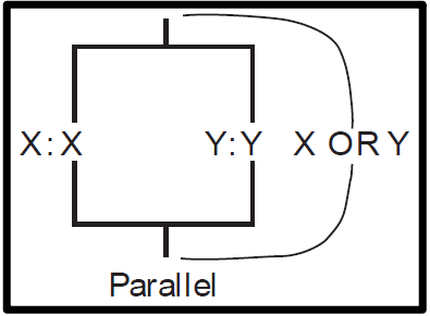
[1] 모두 nMos transistor이며 [2] 이를 Parallel 형태로 연결했으므로
=> X OR Y를 의미합니다. (즉, 둘 중 적어도 하나가 1이어야 연결됩니다.)
3> 결론
transistor로 boolean logic을 구현할 수 있습니다.
3) Fully-Complementary CMOS Circuit

1> 위의 block (F1)
p-type transistor = NC switch
[1] Voltage source로부터 output(F)을 charge
[2] 1을 만들어준다.
[3] p-type transistor 사용
[4] F가 1이 되는 logic
2> 아래 block (F0)
n-type transistor = NO switch
[1] output(F)에 charge된 것을 ground에 연결해서 discharge
[2] 0을 만들어준다.
[3] n-type transistor 사용
[4] F가 0이 되는 logic (F'을 만들면 됩니다.)
4) CMOS Circuit Design Example
1> F를 간소화합니다. F'도 간소화합니다.

2> F0(F')에 해당하는 switch구현 (NO switch로 만든다.)

3> F1(F)에 해당하는 switch 구현 (NC switch 형태로 만든다.)

4> 최종 완성
[1] F1 Circuit
X, Y, Z'가 F1 Circuit에 들어올 때,
p-type transistor여서
F1 Circuit 안에 X', Y', Z가 input으로 주어진 것과 다릅니다.
[2] F0 Circuit
X', Y', Z가 F0 Circuit에 들어올 때,
n-type transistor여서
F0 Circuit 안에 X, Y, Z'가 input으로 주어진 것과 다릅니다.

2. ASIC and CAD
1) ASIC (Application Specific Integrated Circuit)
1> 정의 : 특정 application만 수행하기 위한 IC(chip)
e.g> 닌텐도, mp3 플레이어, 카메라 모듈
2> issue
- volume of sales : 많이 팔아야 하고- fast design time : 설계를 빠르게 할 수 있어야 하고- low design cost : 설계에 적은 비용이 들어가야하고- design quality measured by performance and manufacturing yield : '성능이 괜찮은가'와 '회로가 정상 작동하는가'
2) CAD (Computer-Aided Design)
손으로 설계하면 오류가 많을 수 있으니 computer로 자동화하여 chip을 설계할 수 있다.
1> design 시간을 단축할 수 있고
2> design을 최적화할 수 있습니다.
3. Circuit classification
1) semiconductor material에 따른 분류
1> silicon :
2> Gallium-arsenide : 더 고성능, 가격이 비싸다. e.g> 위성에 쓰인다.
2) electronic device type
1> CMOS(Complementary Metal Oxide Semiconductor) : PMOS & NMOS (일반적인 회로)
2> Bipolar (아날로그적 성격)
3) analog & digital
1> analog circuit : contiuous한 정보를 다룬다. (voltage와 같은 정보를 다룹니다.)
e.g.> 모뎀2> digital circuit : binary한 value를 다룬다. (일반적인 회로)
4) digital circuit 중에 operation 방식에 따른 분류
1> synchronous : global clock이 있습니다. 그래서 전력 소모가 큽니다.2> asynchronous : global clock이 없습니다. 전력 소모가 적습니다. circuit을 control하는 부분이 따로 필요합니다.
5) Microelectronic design style에 따른 분류
1> custom design : functional(high-level) 과 physical(low-level) design을 손으로 design
-> expensive -> design 시간도 오래 걸린다.-> high density, performance design
2> semi-custom : design 시간을 조금 줄이고 성능을 낮춘 형태

4. Circuit design and fabrication
1) Circuit design - Cell based Design
1> Standard-Cell design
[0] Standard-Cell
(큰 것은 저항이 적어서 고성능 고전력)

[1] 위와 같은 Standard Cell들을 만들어두고(Cell generator), library로 저장해둔다.
[2] semiconductor 기술이 발달하면 Standard Cell들을 update한다. (Process Migration)
[3] library binding (technology mapping) : Standard Cell을 조합하여 회로를 설계한다.
2> Hierarchical standard cell design : 작은 cell로 더 큰 cell을 만들어둔다.
3> Macro-cell based design
e.g) RAM, ROM, PLA

장점 : 미리 어느 정도 만들어 두었기 때문에 빨리 만들 수 있습니다.
단점 : 불필요하게 회로가 커질 수 있습니다.
2) Circuit design - Array based Design
1> Prediffused (mask programmable) based design (e.g> Gate array)
2> Prewired (field programmable gate arrays) based design (e.g> Anto-fuse based, memory based)
cf> 각 design 별 특징

3) Circuit Design
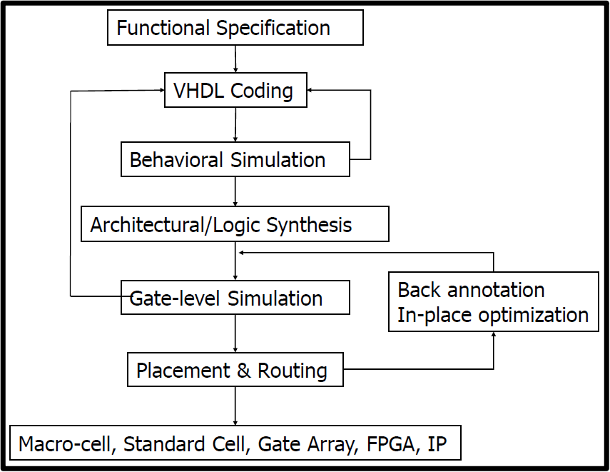
1> design
[1] modeling : HDL로 modeling
[2] synthesis and optimization :
[3] validation : simulation (성능, function이 맞는지), verification (design rule에 맞는지)
2> fabrication
waper에서 한 번에 많은 chip을 만들어냅니다.
4) fabrication
1> Pattern Transfer (lithograph)
[1] CAD로 database를 확보 (이를 final full layout라고 합니다.)
[2] final full layout를 mask maker로 전달
결과적으로 광학적인 방법을 이용해서 patterned wafer를 만듭니다.
2> Selective removal of material (Etching)
wafer에 material을 쌓고
Wet etching(chemical acid)와 Dry etching(plasma, ion miling, RIE)로 필요 없는 material을 제거합니다.

3> Addition of layers
몇몇 재료들 (반도체 재료, metal)을 필요한 만큼만 더해줍니다.
e.g> SiO2 (Oxide), Si3N4 (Nitride), polysilicon, aluminum)
4> Addition of impurities
5> Testing
6> Packaging
- slicing
- packaging
5. Design flow
설계 도면에 가기 전까지 CAD가 하는 것
cf> System-On-Chip

6. Design Constraints
1) Performance
0> Timing analysis
- Entire chip : 시간이 오래 걸릴 수 있다. 그래도 전체 timing performance가 필요한 경우가 있다.
- Critical path : 가장 긴 path
- Block : 작은 단위인 block 단위로 analysis (Divide and Conquer) 그래서 빠르다. 긴 path에서의 주요 정보를 잃을 수 있다.
- Latch : 가장 작은 단위로 analysis할 수 있다.
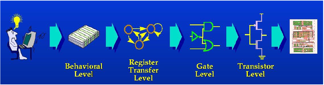
cf> 분석하는 level에 따라 3가지로 분류할 수 있습니다.
3> Transistor(Switch)-Level : 모든 것을 고려해서 timing을 잰다. 시간이 오래 걸리지만 정확하다. (작은 회로에 보통 적용)
2> Logic(Gate)-Level
1> High-Level : 정확하지는 않지만 큰 단위를 분석하는데 적합하다.
1> High-Level Analysis
top-down 방식
2> Logic(Gate)-level Analysis
: circuit delay를 input pin부터 output pin까지 계산해보기
Graph-based formulation 적용 (graph로 변형해서 분석합니다.)
[1] 회로를 graph로 변환하고
[2] pin 1개 = node 1개
[3] delay를 각 node의 weight으로 표기
example>
1번째 pin에서
a는 rising하는데 5만큼 delay, falling하는데 3만큼 delay 발생
b는 rising하는데 3만큼 delay, falling하는데 1만큼 delay 발생
이어지는 2번째 pin에서
rising하는데 5만큼 delay, falling하는데 3만큼 delay 발생

<해설>
rising - pmos
falling - nmos
logic 상 rising과 falling은 각각 연속적으로 등장할 수 없어서 R-S 혹은 S-R 조합으로만 연결되어 있습니다.

=> max delay는 5+3 = 8입니다.
3> Transistor(Switch)-Level
circuit을 양방향 switch로 모델링한다.
[1] Switch level timing analyzer : 간단한 switch로 모델링 e.g> LEADOUT, Pearl, Crystal, PathMill
[2] Circuit level timing analyzer : 정확한 계산을 추구 e.g> SPICE circuit simulation
약 140여개의 equation까지 만들어가며 정확한 계산을 추구
example>

1번째 transistor : input(V_th) = 0 -> 1번째 switch on -> output = 1
-> 2번째 transistor : 2번째 transistor로 1이 들어와서 -> 2번째 switch on -> output (V_pwr) = 1
=> input을 0에서 1로 증가시킵니다.
=> 어느 순간에 1번째 transistor는 연결이 끊어집니다. (빨간 line)
=> 1번째 transistor 아래에 ground가 있었어서 2번째 transistor에 있는 전압이 ground로 빠져나간다.
=> 그래서 2번째 transistor는 0에 가까워집니다.

cf> Timing Macro-modeling technique
[1] Table lookup (or Tabular) delay method : 각 logic gate를 table로 만든다.
input의 slope(빠르게 변하는가 or 느리게 변하는가), output load (wire가 얼마나 있는가)에 따라
여러 library를 만들어둔다.
[2] RC delay and AWE method
[3] Inverter analysis
[4] Nonlinear macro-modeling technique
Nonlinear -> 미분방정식을 푼다는 얘기
cf> Performance Optimization
delay : input에서 output까지의 시간 (delay가 크다는 것 = 느리다)

빠르면 cost가 큽니다. (크고, 비싸고, 전력 소모 크다.)
느리면 cost가 작습니다. (쌉니다.)
=> 최적화할 때, 이 curve를 고려합니다.
2) Power
뜨거우면 성능이 저하된다. (오랫동안 뜨거우면 전자 이동이 느려집니다.)
0> Power는 설계(특히, mobile embedded system)에서 중요한 요인입니다.

(Performance, Power, Area는 각각 서로 비례관계입니다.)
Area ↑ => Performance ↑, Power ↑
Perfornance => Area ↑, Power↑
Power↑ => Area↑, Performance↑
1> Computer Aided Design for power
각 설계 과정마다 power를 측정하고 최적화할 수 있어야합니다.
2> power consumption이 일어나는 경우 3가지
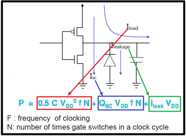
[1] Dynamic Power Consumption (I_load)
input & output이 바뀌는 switching이 일어날 때
(회로 내부가 charging 혹은 discharge될 때)
[2] Short Circuit Current (I_sc)
input이 서서히 바뀔 때(0->1 or 1->0)
순간적으로 Vdd에서 ground로 전류가 조금 빠져나갈 수 있습니다.
example> 위의 예시에서 0이 transistor로 주어지다가 1이 주어진다고 가정합니다.
[3] Leakage (I_leakage)
전류가 새는 경우가 6가지 있습니다.

3> Transistor level power estimation
[1] Circuit level simulation
[2] Switch-level estimation
4> Gate-level power estimation
Dynamic power estimation

5> Gate-level power issue
[1] Capacitance modeling
RLC value를 설계도에서 extract
[2] Glitch modeling
gate delay에 의해 짧은 시간 동안 잘못된 값을 가질 수 있습니다. 이 glitch가 power를 먹는다.
3) Area
4) Testability
5) Design Time
6) Cost
7) Yield
7. Functional verification using OBDD
1) Binary Decision Diagram (BDD)
functional verification에 사용 (원래는 truth table로 검증 but truth table은 너무 size가 큽니다.)
0> 등장 배경
BDD는 canonical (각 boolean function은 unique BDD를 가집니다.) => BDD가 같으면 function이 같다.
BDD는 compact합니다. (multiplier에서만 제외하고)
1> 정의
2> restriction
3> example 1

4> example 2

[1] x1=0 -> x1*x2=0 -> 이 function의 값은 x4에 달려있다. -> BDD가 x1=0 이후에 x4를 거쳐야 한다.
[2] x1=1 -> x1*x2의 값은 x2에 달려있다. -> x1=1 이후에 x2를 거쳐야 한다.
[3] x1=1 & x2=0 -> x1*x2=0 -> 이 function의 값은 x4에 달려있다. x1=0 과 x2=1 이후에는 x4로 가야한다.
[4] x1=1 & x2=1 -> x1*x2=1 -> 이 function의 값은 x4와 상관없이 1이다. -> x4를 거치지 않아도 된다.
2) Ordered Binary Decision Diagram (OBDD)
BDD를 만드는데 input 변수의 순서가 중요하다.
input 변수의 순서를 정해놓고 BDD를 만든다.


